

An AI Engineer's Guide To Choosing GPUs
A deep dive on technical Hardware and Software details of NVIDIA GPUs for AI Workloads.

Welcome to Neural Bits. Each week, I write about practical, production-ready AI/ML Engineering. Join over 7000+ engineers and learn to build real-world AI Systems.
Most AI engineers use NVIDIA GPUs as their compute for AI workloads. Also, most know the names of their GPUs but not the intricate details of the entire picture that matters for a deployable AI System.
From the RTX 3/4/590 everyone trains their LoRA Adapters on, the H100 that powered and still powers LLM clusters, to the new Blackwell B100+ chips entering data centers specifically for Gen AI Training and Inference at scale.
There are a lot of options and configurations. But knowing the name of a GPU will not tell you the most important thing:
GPUs are not monolithic products.
They’re systems composed of layers:
A microarchitecture (e.g., Pascal, Ampere, Hopper, Blackwell) that defines the underlying chip features, which precision formats and tensor features exist etc.
A memory subsystem that determines how fast model weights and activations can move.
A form factor and interconnect (PCIe, SXM, NVLink) that indicate whether GPUs can scale together while using their full capacity.
This guide breaks down the internal logic of NVIDIA’s GPU lineup, as I see it useful from an AI Engineer’s lens:
How does architecture map to capability? How do memory and interconnect constrain or enable AI workloads? And how do consumer GPUs differ from data-center GPUs beyond price and marketing?
To better navigate this article, please use the Table of Contents on the left side.
Fun Personal Story - My First GPU
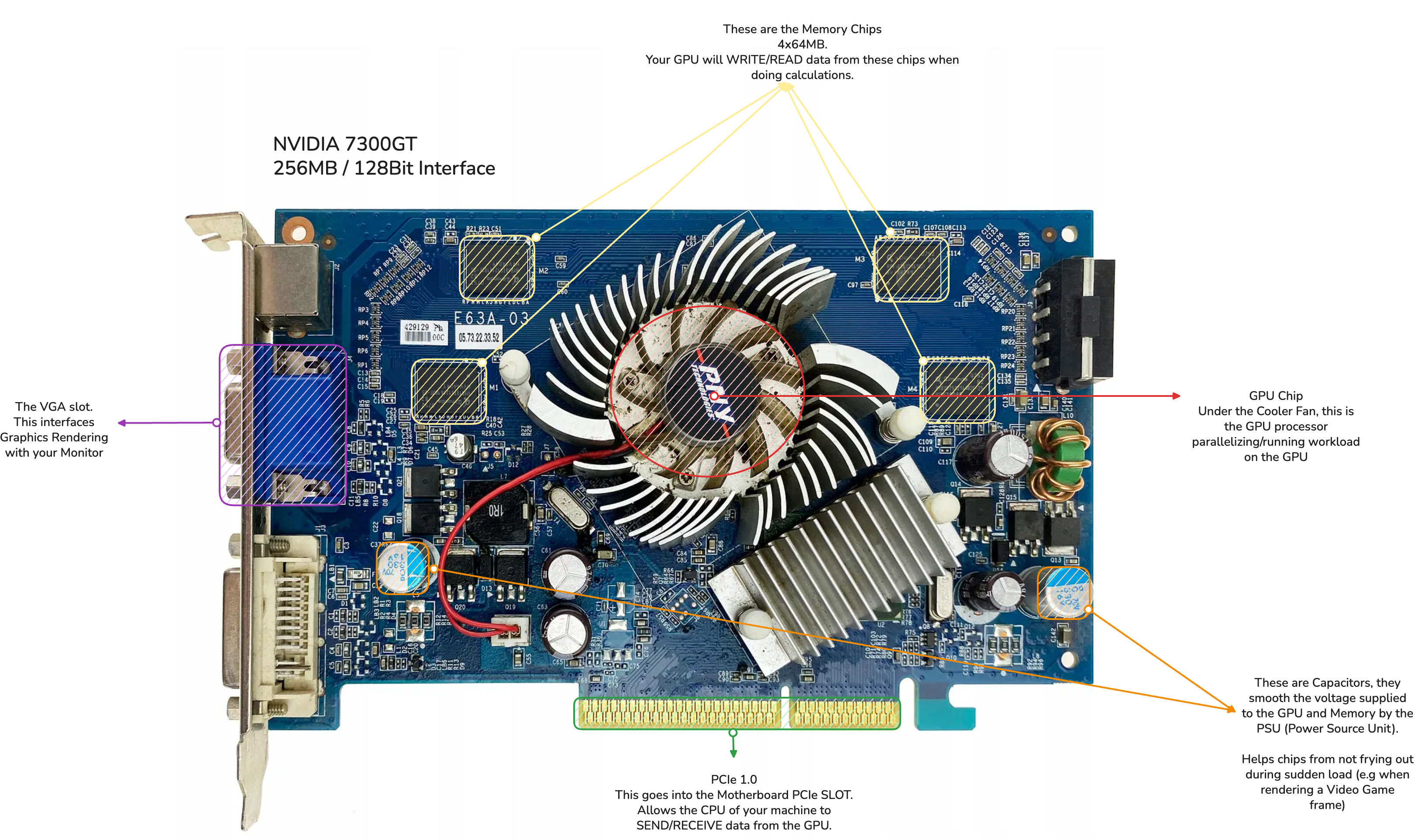
My first ever GPU was an NVIDIA 7300GT, with 256MB VRAM and 128bit BUS. Nowadays, even a microwave is more powerful than this chip was in 2008 when I got it with my first ever Desktop PC my grandmother bought me.
I remember back then, trying to run Grand Theft Auto 4 on my PC, and the game wouldn’t even start, I think rendering the first frame of the Rockstar Games Logo was too much for this little fella. I remember trying to convince my parents to buy me a NVIDIA 9500GT as one of my friends had it and his PC was running the game on High Settings at 1280x1024. That was way over what they could afford at the time.
You could imagine I was spending most of my time at his place whenever I got the chance. In the end, with a lot of tweaks, I’ve managed to play it a bit at 340x280 resolution with everything on Very Low settings, on my own PC.
I remember even modifying the game’s internal .ini files in Windows/ProgramFiles, trying to tweak DirectX 9.0 and disable every Graphics Feature I could find in there, being guided by every tutorial I could find at the time, and after waiting a solid few minutes for pages and videos to load with my Dial-Up internet of 40kb/s via the phone line.
It looked somewhat like this, but with way blurrier pixels, and a 12-13 FPS max, with the GPU Fan working overtime at 70-80 degrees C.
But hey, I could play it. :)

Interestingly enough, It was back then I’ve started to find out NVIDIA SLI, different GPU families, VRAM, memory. I didn’t know or wanted to understand what these were. My complete goal of trying to run this game that everyone at school talked about, on my PC such that I could join the “group”.
Getting back to nowadays, you could easily run way better looking games directly on your phone, at smooth 30+ FPS while not draining your phone battery.
The picture I wanted to paint with this story is that GPUs, Graphics, Supercomputers, AI Compute and technology overall have come a very long way. Now, compute is faster, bigger, more energy efficient and cheaper than ever.
1. Deep Learning Started on 2 x GTX580
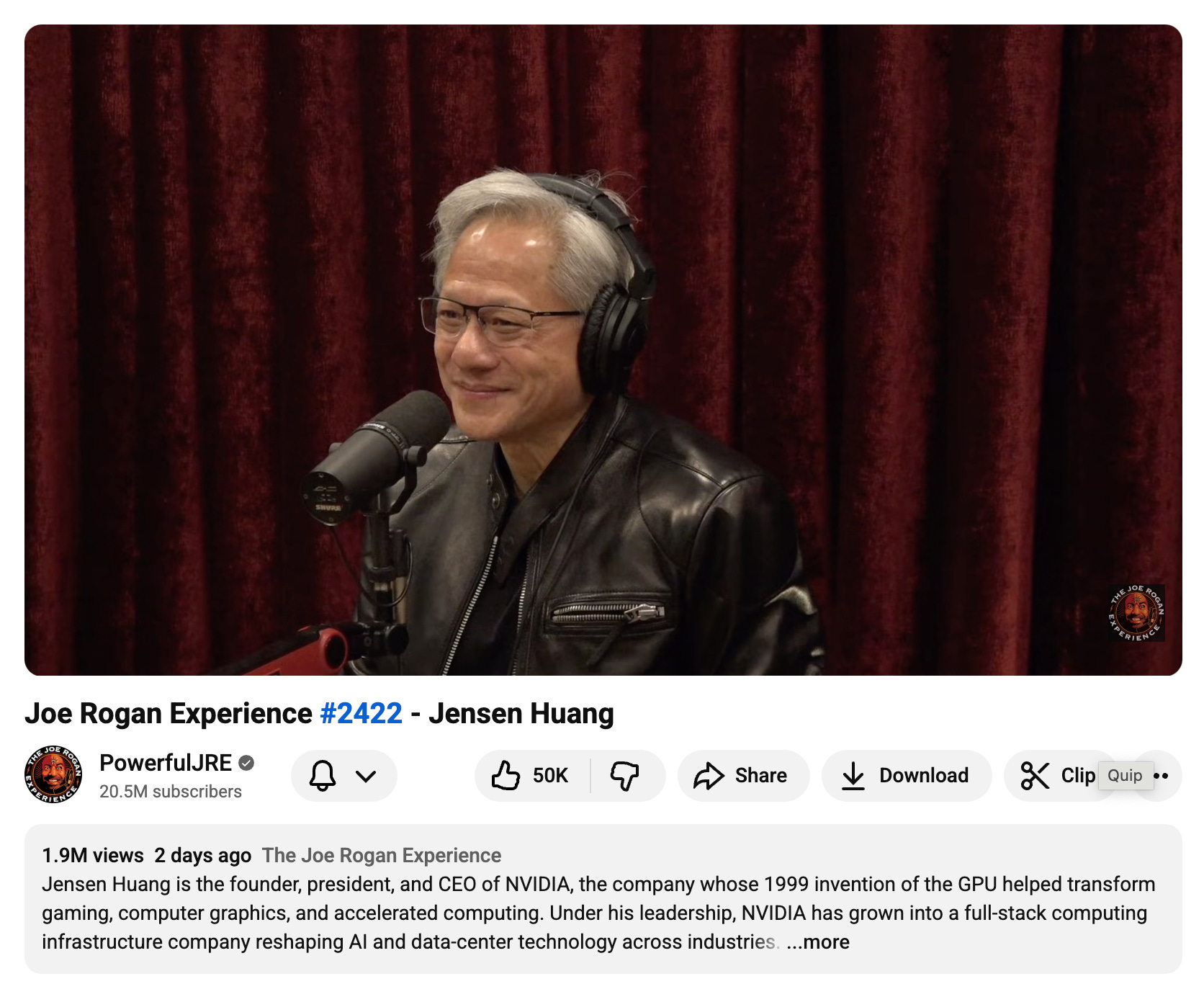
On a recent Joe Rogan podcast episode, Jensen Huang brought up a moment in deep learning history that’s easy to forget now. In 2012, Alex Krizhevsky and Ilya Sutskever trained AlexNet, the Image Classification model that ended up beating all the existing Computer Vision algorithms at the time.
They’ve done that using 2 x NVIDIA GTX 580 gaming GPUs with 3 GB of VRAM each, to build the fast convolutions. That was their whole setup.
The code cuda-convnet was good enough that for several years it was the industry standard and powered the first couple years of the deep learning boom. That success in 2012, hinted that AI progress was going to depend heavily on GPU hardware.
But, hardware is only half of the slice. If you write or deploy modern AI models, you’re almost certainly doing it on NVIDIA hardware. That’s not just about FLOPs or how large the GPU VRAM is, equally important is the Software stack, the low-level libraries, frameworks and SDKs that allow AI Engineers to train, optimize and deploy their AI Models.
As an AI engineer, your life is much easier if you understand how NVIDIA organizes its GPU stack.
This piece is a practical map of that stack, starting Hardware First.
Software view: compute capability and CUDA features
Architecture view: Ampere → Hopper → Blackwell
Hardware view: PCIe vs SXM, NVLink, and when they matter
2. Understanding Compute Capability
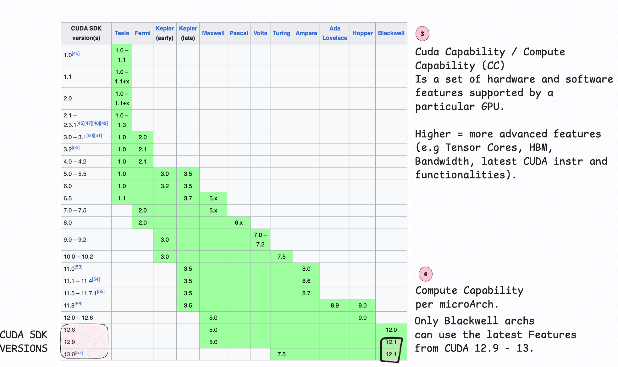
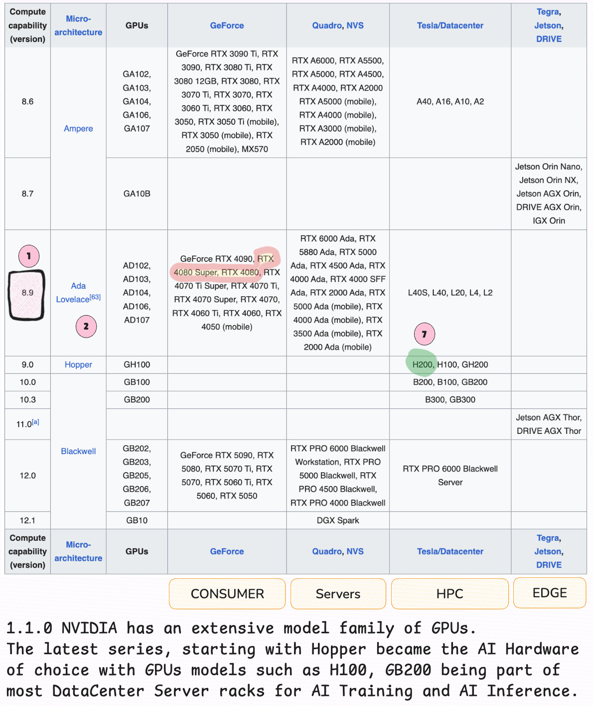
Every NVIDIA GPU has a Compute Capability (CC) like 7.0, 8.9, 9.0, etc. This number defines which instructions, cuda cores, tensor cores, memory ops, and features a GPU supports. Simply put, the CC number defines the set of hardware features per GPU architecture.
For instance, if we analyze this table, we’ll see the CC number associated with each family of GPU Chips, from the older Tesla GPUs, up to the latest Blackwell chip designed for AI.
The GT7300 I’ve had in 2008, was part of the Tesla family of architectures. Interestingly enough a slightly modified version of a Tesla-family GPU, the 7800GTX, called (RSX) Reality Synthesizer was used in Playstation 3.
That chip was developed jointly by Sony and NVIDIA.
If you own an NVIDIA GPU, you can see the CC via running this in your terminal:
nvidia-smi --query-gpu=name,compute_cap --format=csv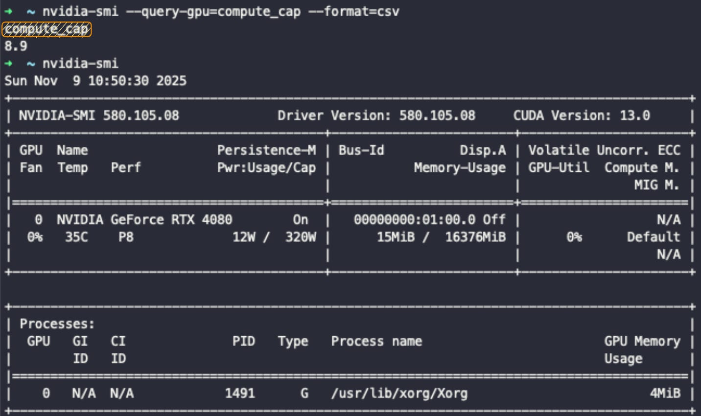
A few things are tightly coupled to compute capability:
Tensor Cores & precision formats
Ampere (A100, RTX 30XX): TF32 + FP16 Tensor Cores
Hopper (H100): adds FP8 via the Transformer Engine.
Blackwell (B100/B200): pushes further to FP4/NVFP4 for inference.
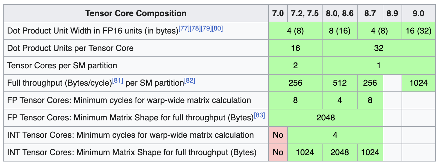
Memory - Newer CCs support HBM2E/HBM3/HBM3e, larger memory, and faster NVLink generations.
CUDA & library support - At some point, new CUDA features stop backporting to older CCs.
The rule of thumb when analyzing GPUs is the higher the CC, the more “native” support you get for modern AI features (FP8/FP4, better sparsity, bigger memory, new interconnects). The following diagram is an overview on GPU Architecture families and models, from Consumer GPUs to Data Center GPUs, and how these are tied to the Compute Capability score.
To summarize this section, Compute Capability tells you which hardware features a GPU actually supports, and whether your kernels will run at full speed. VRAM, FLOPs, and interconnect matter but only after the capability makes those features usable.
After CC, the next layer into understanding a GPU’s Performance is the Technical Cheatsheet, from where we extract details such as connectors, FLOPs, Bandwidth Memory and more.
3. Understanding a Technical Cheatsheet
After understanding CC, a GPU cheatsheet is another key reference tool for an AI engineer to understand hardware and software optimization details. In a Technical Cheatsheet, an engineer will find the metrics on CPU Performance, power usage, number of FLOPs in different precision formats (FP32/FP16) and the GPU form factor.
The latter is important for building compute clusters, where multiple GPUs have to be connected and share the resource pool. A cheatsheet allows you to quickly answer some of these questions:
Will this GPU support the precision modes?
Does it have enough VRAM and Bandwidth?
Is inter-GPU bandwidth high enough for model parallelism?
Will this deploy cleanly in my existing hardware stack?
In the following image, let’s inspect the Technical Cheatsheet for the Hopper H200 GPU, covering a few key details on FLOPs and explain the difference between the form factors such as SXM or PCIe.
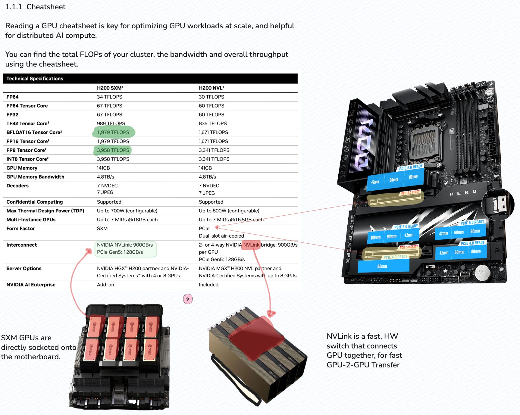
From the cheatsheet, an AI Engineer would likely look first at the GPU Memory, Bandwidth and FLOPS for a specific Precision Type which directly impacts the speed of AI model training and inference.
For this specific GPU model, a single H200 GPU features 141GB of memory, with a 4.8TB/s bandwidth. For Vision based workloads, that maybe imply real-time vision AI inference, this GPU features NVDEC which allows for video decoding and feeding data as tensor-ready structures instead of it passing through the CPU.
MIG - Multi Instance GPU
Another important detail is MIG (Multi Instance GPU) which allows engineers to shard a single physical GPU into multiple instances of virtual GPUs, each in an isolated space.
For instance, a single H200 could be split into 4 MIG instances, each one with 36GB of VRAM. That means 4 different AI Engineers, could work in separated environments each with their own workload.
Think of a multi-agent system, with multiple LLM models in their own VRAM and GPU boundary working simultaneously on different tasks.
During experimentation of model training phase, MIG also could come in handy to run the same experiment with multiple configurations or optimization profiles. A MIG instance could quantize to FP8 and inference with a 32 batch size, and another could quantize to FP4 and inference batch size 64.
Form Factor - SXM or PCIe
Let’s focus on the form-factor, as this also impacts the GPU performance. In this cheatsheet, there are 2 form factors PCIe and SXM. The PCIe (Peripheral Component Interconnect Express) is an interface standard that is common for consumer GPUs.
In the attached image, there is a Gaming PC Motherboard, featuring a PCIe 5.1 slot for the GPU, think RTX4080/4090/5090. On the other hand, SXM is a special chip embedded into the motherboard directly, and used in DataCenter clusters.
For example an H200 DGX Server contains 8 x H200 GPUs. These are not connected via PCIe, but on SXM directly and connected via NVLink.
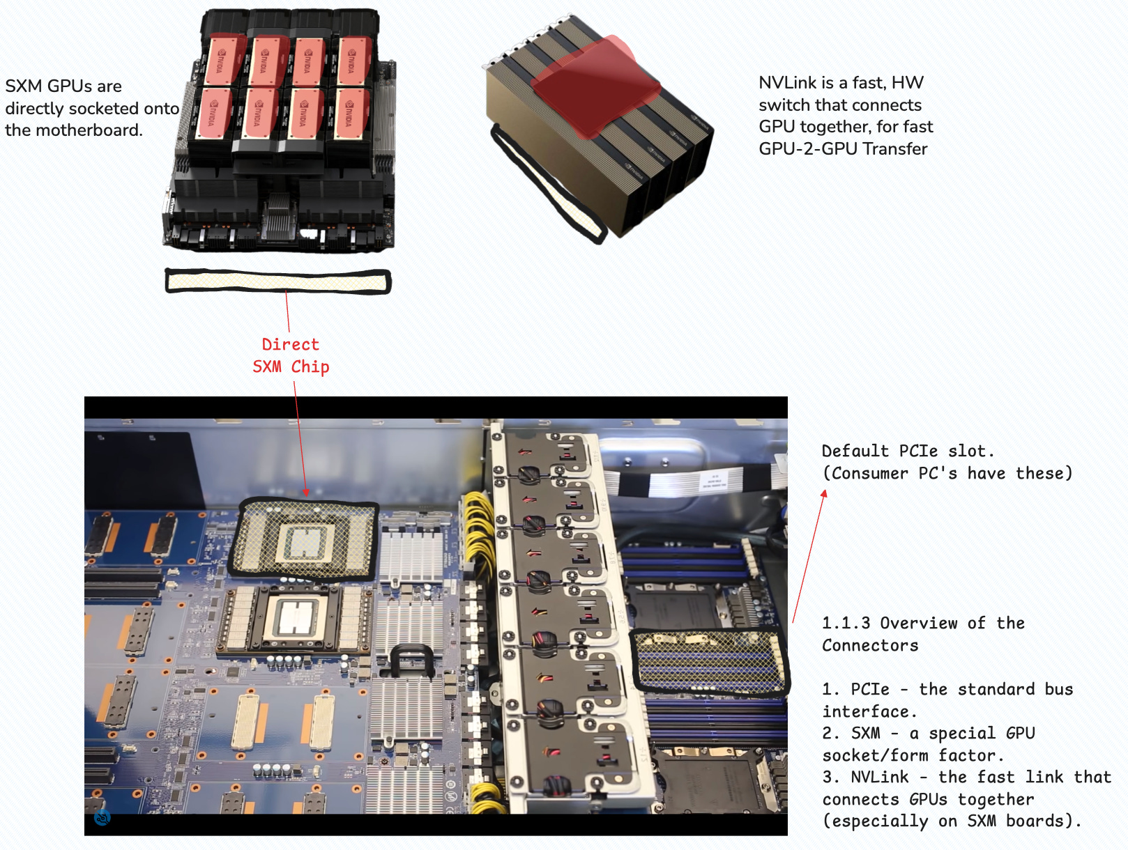
With SXM, you get higher power input which mean higher sustained clock speeds and direct GPU-GPU links through the NVLink switches. This is important for training or serving large models as AI Engineers could use the full benefits of parallelization techniques such as Tensor Parallel or Pipeline Parallel with low latency in GPU-GPU communication.
For example, the H100 SXM variants can participate in NVLink/NVSwitch topologies where 16 GPUs share hundreds of GB/s of bidirectional bandwidth. Multi-GPU clusters are generally used for training and inferencing large dense LLMs and MoE Models as token exchanges and activations in MoE networks require fast GPU-GPU communication.

What is NVLink
To understand NVLink and NVSwitch, we could first look at the older connector called SLI. The 2xGTX550 that were used to train AlexNet in 2012 were routed using the SLI Bridge to enable faster computation and data sharing between the two. SLI came during the era of Gaming, during which NVIDIA was selling consumer-first GPUs to render graphics.

NVLink is the successor of the SLI, targeting AI workloads.
For Desktops (PCIe Cards): NVLink is connected using a physical external bridge called an NVLink Bridge. This is a compact, solid PCB-based connector that plugs into dedicated NVLink ports on the top edge of two adjacent GPU cards, similar to the older SLI bridge.
For Servers (SXM Modules): In high-density server environments (like NVIDIA’s DGX systems), the NVLink connections are integrated directly into the multi-GPU baseboard. The GPU modules (SXM form factor) plug into this baseboard, making the physical NVLink connection an internal part of the server structure.
For instance, below is an image of 2 x A100 PCIe GPUs, connected with NVLink bridges.

4. How to Choose a GPU as an AI Engineer
A typical AI engineering workflow is highly dependent on specialized hardware to accelerate model training and inference. While the majority of this work sources on cloud compute platforms, many teams, especially those dealing with extremely sensitive data or specialized needs, still utilize on-premise compute clusters. Regardless of the deployment environment, the decision on which GPU to use should be based on a well researched plan.
The common deployment environments for AI engineers are:
Cloud Compute: Services like AWS, Azure, GCP or natively NVIDIA DGX Cloud offer scalable, pay-as-you-go access to top-tier hardware (e.g., NVIDIA H100s). Niche providers like LambdaCloud or RunPod also offer compelling alternatives.
On-Premise Labs: Engineers working in private data centers or dedicated labs have full control over the hardware, often using NVIDIA DGX or HGX systems.
On-premise is the current pick for most AI Labs out there, OpenAI, Anthropic, X and Meta, they all bought DGX Clusters or large orders of GPUs from NVIDIA to build their own data centers.
That’s because in most AI Research, and you might run 100 experiments from which 70 failed, and paying for on-demand resources, cold start, provisioning on large cloud clusters gets quite expensive.
When comparing specific GPU SKUs, whether in the cloud or on-premise engineers often evaluate them based on three technical pillars:
Compute Capability (Hardware and Software)
For NVIDIA, the CC metric dictates the low-level features a GPU supports, covering Precision Types, Tensor Core or CUDA Cores configurations.
Usable Memory (VRAM & Bandwidth)
VRAM is the amount of memory available, and bandwidth is how fast data can be moved in and out of it. Although LLMs tend to get smaller and be quite good at 12B, 30B parameters, loading such models in memory in their pre-training BF16 precision requires a lot of VRAM.
Bandwidth is another key performance aspect. Training or fine tuning LLMs imply multiple RW operations that involve all of the GPUs memory, not only it’s VRAM. A GPU also has SRAM and Registers which are used whenever data computed by a kernel needs to be cached for the execution of another kernel, or copied back to VRAM and made accessible to the CPU.
Most last-gen GPUs have HBM (High Bandwidth Memory) which is more tuned for AI workloads than the GDDR-X memory used for consumer-grade GPUs.
Interconnect (Communication)
This defines how fast GPUs can communicate with each other, which is crucial for distributed training as most models are not trained or fine-tuned on a single GPU, but often involve a multi GPU cluster.
Note: Mistral 8x7B MoE was trained from scratch on 240 x H100 GPUs which, with this kind of setup being similar in most LLM pre-training runs.
The key difference to make here is the connection interface, choosing between PCIe standard or SXM and NVLink, with the later being the go-to for large scale LLM training in distributed setups.
Evaluating a GPU option following these three pillars, across software capability, memory, and interconnect would filter the GPU options one is selecting from, and allowing you to tune the system after the specific requirements of your workloads.
5. Closing Thoughts
The AI world moves fast, but the underlying questions don’t change:
Can my GPU run the kernels I need? → CC and Architecture
Can I fit my model and batch size? → VRAM & Memory Type & Bandwidth
Can my GPUs communicate fast enough? → PCIe & SXM
Ultimately, the right choices for an AI engineer comes down to matching these core needs to the right tool, ecosystem and scalability requirements. Establishing the range of requirements for the AI Workload you’re working on (pre-training, fine tuning or inference) would simplify the process of selecting the right compute by a lot.
Thank you for reading, if you’ve enjoyed this article, consider subscribing for free.